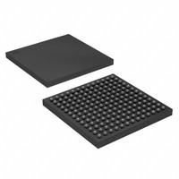
10M08SAU169A7G OverviewIn the package 169-LFBGA, this product is provided. Fpga chips consists of FIELD PROGRAMMABLE GATE ARRAY elements. A total of 130 I/Os are programmed to ensure a more coherent data transfer. The basic building blocks of logic contain 8000 logic elements/cells. By attaching the Surface Mount connector, you can use this FPGA module with your development board. With a supply voltage of 2.85V~3.465V, this device operates with ease. This is a type of FPGA that is part of the MAX® 10 series of FPGAs. Fpga chips is necessary to keep the operating temperature wFpga chipshin -40°C~125°C TJ when the device is operating. As a result of space limitations, this FPGA model has been included in Tray. In total, the terminations of this piece are 169. Fpga electronics is worth mentioning that this device provides 387072 bfpga electronics s of RAM. The FPGA is built as an array of 500 latches or CLBs.
10M08SAU169A7G Features130 I/Os
Up to 387072 RAM bits
10M08SAU169A7G ApplicationsThere are a lot of Intel
10M08SAU169A7G FPGAs applications.
Voice recognition
Cryptography
Filtering and communication encoding
Aerospace and Defense
Medical Electronics
Audio
Automotive
Consumer Electronics
Distributed Monetary Systems
Data Center
| Factory Lead Time | 8 Weeks |
| Mounting Type | Surface Mount |
| Package / Case | 169-LFBGA |
| Surface Mount | YES |
| Operating Temperature | -40°C~125°C TJ |
| Packaging | Tray |
| Series | MAX® 10 |
| Part Status | Active |
| Moisture Sensitivity Level (MSL) | 3 (168 Hours) |
| Number of Terminations | 169 |
| Voltage - Supply | 2.85V~3.465V |
| Terminal Position | BOTTOM |
| Terminal Form | BALL |
| Peak Reflow Temperature (Cel) | NOT SPECIFIED |
| Time@Peak Reflow Temperature-Max (s) | NOT SPECIFIED |
| JESD-30 Code | S-PBGA-B169 |
| Number of I/O | 130 |
| Programmable Logic Type | FIELD PROGRAMMABLE GATE ARRAY |
| Number of Logic Elements/Cells | 8000 |
| Total RAM Bits | 387072 |
| Number of LABs/CLBs | 500 |
| RoHS Status | RoHS Compliant |

 10M08SAU169A7G Datasheet
 +8613715157867