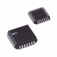
AD569JP OverviewA 28-LCC (J-Lead) package is provided with this component. An electrical supply voltage of 12V powers it. An FPGA module can be attached to a development board with a Surface Mount-pin. During the operation of the system, the operating temperature should remain within the range of 0°C~70°C. It is for space saving reasons that this FPGA model is contained in Tube. As a whole, it has 28 terminations. Related parts can be found by using its base part number AD569. 28 pins are designed into the device. As long as this FPGA is mounted in Surface Mount, it should be able to function as it should in terms of its specifications, as well as its capabilities. In addition to this, it has 28 pins. A maximum voltage of 13.2V can be supplied to it. As long as the supply voltage is at least 10.8V, it is able to work properly.
AD569JP Features28-LCC (J-Lead) package
28 pin count
28 pins
AD569JP ApplicationsThere are a lot of Analog Devices Inc.
AD569JP Digital to Analog Converters (DAC) applications.
Data Distribution System
Digital Potentiometer
Software Radio
Wireless infrastructure:
WCDMA, CDMA2000, TD-SCDMA, WiMAX
Wideband communications:
LMDS/MMDS, point-to-point
Instrumentation:
RF signal generators, arbitrary waveform generators
Mobile Communications
| Contact Plating | Lead, Tin |
| Mount | Surface Mount |
| Mounting Type | Surface Mount |
| Package / Case | 28-LCC (J-Lead) |
| Number of Pins | 28 |
| Operating Temperature | 0°C~70°C |
| Packaging | Tube |
| JESD-609 Code | e0 |
| Pbfree Code | no |
| Part Status | Obsolete |
| Moisture Sensitivity Level (MSL) | 1 (Unlimited) |
| Number of Terminations | 28 |
| ECCN Code | EAR99 |
| Max Power Dissipation | 1W |
| Terminal Position | QUAD |
| Terminal Form | J BEND |
| Peak Reflow Temperature (Cel) | 225 |
| Number of Functions | 1 |
| Supply Voltage | 12V |
| Time@Peak Reflow Temperature-Max (s) | 30 |
| Base Part Number | AD569 |
| Pin Count | 28 |
| Output Type | Voltage - Buffered |
| Polarity | Bipolar, Unipolar |
| Max Supply Voltage | 13.2V |
| Min Supply Voltage | 10.8V |
| Nominal Supply Current | 9mA |
| Number of Bits | 16 |
| Architecture | Segmented DAC |
| Converter Type | D/A CONVERTER |
| Reference Type | External |
| Data Interface | Parallel |
| Differential Output | No |
| Resolution | 2 B |
| Voltage - Supply, Analog | ±10.8V~13.2V |
| Settling Time | 6μs |
| Max Dual Supply Voltage | 13.2V |
| Linearity Error-Max (EL) | 0.04% |
| Min Dual Supply Voltage | 10.8V |
| Input Bit Code | BINARY |
| Dual Supply Voltage | 12V |
| Number of Converters | 1 |
| INL/DNL (LSB) | ±0.02, ±0.5 |
| Negative Supply Voltage-Nom | -12V |
| Analog Output Voltage-Max | 5V |
| Analog Output Voltage-Min | -5V |
| Height Seated (Max) | 4.57mm |
| RoHS Status | Non-RoHS Compliant |
| Lead Free | Contains Lead |

 AD569JP Datasheet
 +8613715157867