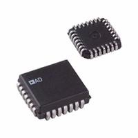
AD7547KP OverviewThere are two packages that contain it: 28-LCC (J-Lead) package and X package. The supply voltage is 12V volts. An attachment Surface Mount allows the FPGA module to be attached to the development board. When operating the machine, it is important to keep the temperature within -40°C~85°C range. There is an FPGA model contained in Tube in order to conserve space. In total, it has 28 terminations on each end. In order to find related parts, use the part number AD7547 as a base. In this case, there are 28 pins on the board. This device has a pin count of 28 in it. A maximum supply voltage of 16.5V can be applied to this product. The minimal supply voltage required for it is 10.8V.
AD7547KP Features28-LCC (J-Lead) package
28 pin count
28 pins
Minimal input voltage of 10V
AD7547KP ApplicationsThere are a lot of Analog Devices Inc.
AD7547KP Digital to Analog Converters (DAC) applications.
Digital Potentiometer
Software Radio
Wireless infrastructure:
WCDMA, CDMA2000, TD-SCDMA, WiMAX
Wideband communications:
LMDS/MMDS, point-to-point
Instrumentation:
RF signal generators, arbitrary waveform generators
Mobile Communications
Process Control and Industrial Automation
| Contact Plating | Lead, Tin |
| Mounting Type | Surface Mount |
| Package / Case | 28-LCC (J-Lead) |
| Surface Mount | YES |
| Number of Pins | 28 |
| Operating Temperature | -40°C~85°C |
| Packaging | Tube |
| JESD-609 Code | e0 |
| Pbfree Code | no |
| Part Status | Obsolete |
| Moisture Sensitivity Level (MSL) | 1 (Unlimited) |
| Number of Terminations | 28 |
| ECCN Code | EAR99 |
| Terminal Finish | Tin/Lead (Sn85Pb15) |
| Terminal Position | QUAD |
| Terminal Form | J BEND |
| Peak Reflow Temperature (Cel) | 225 |
| Number of Functions | 2 |
| Supply Voltage | 12V |
| Time@Peak Reflow Temperature-Max (s) | 30 |
| Base Part Number | AD7547 |
| Pin Count | 28 |
| Output Type | Current - Unbuffered |
| Max Supply Voltage | 16.5V |
| Min Supply Voltage | 10.8V |
| Power Dissipation | 30mW |
| Number of Bits | 12 |
| Max Output Voltage | 20V |
| Min Input Voltage | 10V |
| Architecture | R-2R |
| Max Input Voltage | -10V |
| Converter Type | D/A CONVERTER |
| Reference Type | External |
| Data Interface | Parallel |
| Differential Output | No |
| Resolution | 1.5 B |
| Sampling Rate | 667 ksps |
| Voltage - Supply, Analog | 10.8V~16.5V |
| Min Output Voltage | 0V |
| Voltage - Supply, Digital | 10.8V~16.5V |
| Settling Time | 1.5μs |
| Integral Nonlinearity (INL) | 0.5 LSB |
| Input Bit Code | BINARY |
| Conversion Rate | 667 ksps |
| INL/DNL (LSB) | ±0.5 (Max), ±1 (Max) |
| Number of DAC Channels | 2 |
| Length | 11.506mm |
| Height Seated (Max) | 4.57mm |
| Width | 11.506mm |
| RoHS Status | Non-RoHS Compliant |
| Lead Free | Contains Lead |

 AD7547KP Datasheet
 +8613715157867