CDCM61001RHBR OverviewA clock integrated circuit is packaged in a Tape & Reel (TR)-shaped package because it is for use as a clock. There is a clock generator embedded in the 32-VFQFN Exposed Pad package. This clock generator will sustain a maximum temperature of 260 when reflown. There are 32 terminations found in the file. The clock generator ic should be grounded with a voltage of 3.3V. This clock generator receives its inputs from LVCMOS, Crystal, which is designed to be the clock source. An upper frequency limit of 683.28MHz Max can be achieved with this clock-based frequency synthesizer. Due to the Surface Mount-shape, this electronic component can be conveniently installed on the panel. Approximately 3.6V is the maximum supply voltage needed by this time clock generator. It is safe to use this frequency synthesizer with a supply voltage above 3V. As long as there are 3V~3.6V supply voltages provided, clock generator ic should work. Statistics suggest that the ambient temperature be set at -40°C~85°C, which is what is estimated by the test. It's compatible with LVCMOS, LVDS, LVPECL logic levels. As far as electrical parts go, this component can be classified as a Clock Generator component. There is a 32-bit clock-generating IC built specifically for microprocessors in this frequency generator. These related electrical parts are available for the base part number CDCM61001. PLL is designed with 32 pins. The supply voltage should be maintained at 3.3V for high efficiency. The output frequency can be amplified as high as possible with its 1 signal outputs. The load capacitance is 5pF. Ideally, this electronic frequency generator fits the TR package.
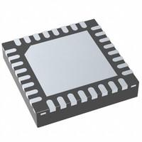
CDCM61001RHBR FeaturesAvailable in the 32-VFQFN Exposed Pad
Supply voltage of 3.3V
Operating supply voltage of 3.3V
Load capacitance of 5pF
CDCM61001RHBR ApplicationsThere are a lot of Texas Instruments
CDCM61001RHBR Clock Generators applications.
Wireless infrastructure
Instrument
Automatic test equipment
Wide area power system
Digital circuits
Wireless base station for LTE, LTE-advanced
Picocells, femtocells and small cells
Sampling clocks for ADC and DAC
1 Gigabit Ethernet
10 Gigabit Ethernet
| Lifecycle Status | ACTIVE (Last Updated: 3 days ago) |
| Factory Lead Time | 16 Weeks |
| Contact Plating | Gold |
| Mount | Surface Mount |
| Mounting Type | Surface Mount |
| Package / Case | 32-VFQFN Exposed Pad |
| Number of Pins | 32 |
| Operating Temperature | -40°C~85°C |
| Packaging | Tape & Reel (TR) |
| JESD-609 Code | e4 |
| Pbfree Code | yes |
| Part Status | Active |
| Moisture Sensitivity Level (MSL) | 2 (1 Year) |
| Number of Terminations | 32 |
| Type | Clock Generator |
| Packing Method | TR |
| Voltage - Supply | 3V~3.6V |
| Terminal Position | QUAD |
| Peak Reflow Temperature (Cel) | 260 |
| Number of Functions | 1 |
| Supply Voltage | 3.3V |
| Base Part Number | CDCM61001 |
| Output | LVCMOS, LVDS, LVPECL |
| Pin Count | 32 |
| Number of Outputs | 1 |
| Operating Supply Voltage | 3.3V |
| Supply Voltage-Max (Vsup) | 3.6V |
| Supply Voltage-Min (Vsup) | 3V |
| Load Capacitance | 5pF |
| Nominal Supply Current | 95mA |
| Frequency (Max) | 683.28MHz |
| Input | LVCMOS, Crystal |
| Ratio - Input:Output | 1:2 |
| PLL | Yes with Bypass |
| Differential - Input:Output | No/No |
| Divider/Multiplier | Yes/No |
| fmax-Min | 683.264 MHz |
| Height | 1mm |
| Length | 5mm |
| Width | 5mm |
| Thickness | 900μm |
| Radiation Hardening | No |
| RoHS Status | ROHS3 Compliant |
| Lead Free | Lead Free |


 +8613715157867