CDCVF2509APWRG4 OverviewClock ICs are packaged using the Tape & Reel (TR) method. In the 24-TSSOP (0.173, 4.40mm Width) package, there is an embedded clock generator. A maximum temperature of 260 can be sustained by this clock generator ic during reflowing. There are a total of 24 terminations in this file. A voltage of 3.3V should be applied to this electronic frequency generator. In this case, LVTTL is designed to be the input of the clock generator. To access the electronic component's full performance, 1 circuits are implemented. The frequency generator has a maximum frequency of 175MHz. Thanks to the Surface Mount, this electric component can easily be installed on a panel. There is a maximum voltage of 3.6V for this clock generator. Keeping the supply voltage for this frequency synthesizer above 3V is recommended for safety reasons. There are 3V~3.6V available for use with this clock PLL. Test statistics suggest setting the ambient temperature at 0°C~85°C, which is 0°C~85°C. It is possible to classify this electronic component as a PLL Clock Driver. An IC that generates clocks specifically for microprocessors, this clock PLL is 24-bits in si24e. The related electrical components for the base part number CDCVF2509 can be found below. A 24 pin is available on the clock PLL. Clock PLL is capable of handling a voltage of 3.3V. The output frequency is magnified as high as possible with 9 signal outputs. Depending on the load capacitance, the analog clock generator can deliver a value of 25pF. There is no doubt that the TR package is an ideal fit for this clock generator ic.
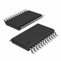
CDCVF2509APWRG4 FeaturesAvailable in the 24-TSSOP (0.173, 4.40mm Width)
Supply voltage of 3.3V
Operating supply voltage of 3.3V
Load capacitance of 25pF
CDCVF2509APWRG4 ApplicationsThere are a lot of Texas Instruments
CDCVF2509APWRG4 Clock Generators applications.
Wide area power system
Digital circuits
Wireless base station for LTE, LTE-advanced
Picocells, femtocells and small cells
Sampling clocks for ADC and DAC
1 Gigabit Ethernet
10 Gigabit Ethernet
FPGA and processor clocks
Line cards used in telephone exchange
Fiber Channel
| Lifecycle Status | ACTIVE (Last Updated: 3 days ago) |
| Factory Lead Time | 6 Weeks |
| Contact Plating | Gold |
| Mount | Surface Mount |
| Mounting Type | Surface Mount |
| Package / Case | 24-TSSOP (0.173, 4.40mm Width) |
| Number of Pins | 24 |
| Weight | 89.499445mg |
| Operating Temperature | 0°C~85°C |
| Packaging | Tape & Reel (TR) |
| JESD-609 Code | e4 |
| Pbfree Code | yes |
| Part Status | Active |
| Moisture Sensitivity Level (MSL) | 1 (Unlimited) |
| Number of Terminations | 24 |
| Type | PLL Clock Driver |
| Packing Method | TR |
| Voltage - Supply | 3V~3.6V |
| Terminal Position | DUAL |
| Terminal Form | GULL WING |
| Peak Reflow Temperature (Cel) | 260 |
| Number of Functions | 1 |
| Supply Voltage | 3.3V |
| Terminal Pitch | 0.65mm |
| Base Part Number | CDCVF2509 |
| Pin Count | 24 |
| Number of Outputs | 9 |
| Operating Supply Voltage | 3.3V |
| Supply Voltage-Max (Vsup) | 3.6V |
| Supply Voltage-Min (Vsup) | 3V |
| Number of Circuits | 1 |
| Load Capacitance | 25pF |
| Power Dissipation | 700mW |
| Frequency (Max) | 175MHz |
| Output Characteristics | SERIES-RESISTOR |
| Input | LVTTL |
| Ratio - Input:Output | 2:10 |
| PLL | Yes with Bypass |
| Differential - Input:Output | No/No |
| Height | 1.2mm |
| Length | 7.8mm |
| Width | 4.4mm |
| Thickness | 1mm |
| Radiation Hardening | No |
| RoHS Status | ROHS3 Compliant |
| Lead Free | Lead Free |

 CDCVF2509APWRG4 Datasheet
 +8613715157867