PCKV857ADGV,118 OverviewThe package Tape & Reel (TR) includes it. In order to ensure the safety and security of the product, it is packaged in a case with a 48-TFSOP (0.173, 4.40mm Width)-serial number. In general, Surface Mount is recommended as the mounting type. This termination has 48 terminations. 2.5V is the voltage provided by this part. 260 runs using this part's peak reflow temperature. In the device, there are 1. Clock program is normalfor the operation frequency to be 250MHz. Vsup reaches 2.7V at its maximum. In order to guarantee normaloperation, the supply voltage (Vsup) needs to be above 2.3V. There is a wide range of operating temperatures for 0°C~70°C. Components can produce voltages of 2.3V~2.7V. Its main function is Memory, DDR, SDRAM. A total of 2003 publications have been made of the part. In order to search for information, you will use the base part number PCKV857. The board contains 48 pins. There are PLL BASED CLOCK DRIVER logic IC types used in it.
PCKV857ADGV,118 FeaturesMounting Type: Surface Mount
Peak Reflow Temperature (Cel): 260
Include 1 Circuits
Logic IC Type: PLL BASED CLOCK DRIVER
PCKV857ADGV,118 ApplicationsThere are a lot of NXP USA Inc.
PCKV857ADGV,118 application specific timer applications.
Processor and FPGA clocking
Any-frequency clock conversion
MSAN/DSLAM/PON
Fibre Channel, SAN
Telecom line cards
1 GbE and 10 GbE
Servers, Storage, Search Acceleration
Ethernet Switches, Routers
Small Cells, Mobile Backhaul/Fronthaul
Print Imaging
| Mounting Type | Surface Mount |
| Package / Case | 48-TFSOP (0.173, 4.40mm Width) |
| Surface Mount | YES |
| Operating Temperature | 0°C~70°C |
| Packaging | Tape & Reel (TR) |
| Published | 2003 |
| Part Status | Obsolete |
| Moisture Sensitivity Level (MSL) | 1 (Unlimited) |
| Number of Terminations | 48 |
| Voltage - Supply | 2.3V~2.7V |
| Terminal Position | DUAL |
| Terminal Form | GULL WING |
| Peak Reflow Temperature (Cel) | 260 |
| Number of Functions | 1 |
| Supply Voltage | 2.5V |
| Terminal Pitch | 0.4mm |
| Reach Compliance Code | unknown |
| Time@Peak Reflow Temperature-Max (s) | 40 |
| Base Part Number | PCKV857 |
| Pin Count | 48 |
| JESD-30 Code | R-PDSO-G48 |
| Qualification Status | Not Qualified |
| Supply Voltage-Max (Vsup) | 2.7V |
| Supply Voltage-Min (Vsup) | 2.3V |
| Number of Circuits | 1 |
| Frequency (Max) | 250MHz |
| Input | SSTL-2 |
| Ratio - Input:Output | 1:10 |
| Logic IC Type | PLL BASED CLOCK DRIVER |
| PLL | Yes |
| Differential - Input:Output | Yes/Yes |
| Main Purpose | Memory, DDR, SDRAM |
| Number of True Outputs | 10 |
| Length | 9.7mm |
| Width | 4.4mm |
| RoHS Status | ROHS3 Compliant |
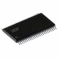

 PCKV857ADGV,118 Datasheet
 +8613715157867